Scientists at Los Alamos National Laboratory They are developing nanometer-scale light-based systems that lead to advances in ultrafast microelectronics, room-temperature infrared detection (for example, night vision), and a wide range of technological applications.
Much of modern technology, from computers to applications such as energy harvesting, is built on the ability to push electrons around. But the way we control this charge flow is very limited by conventional materials and structures.
Jacob Pettin, Physicist, Center for Integrative Nanotechnologies, Los Alamos National Laboratory
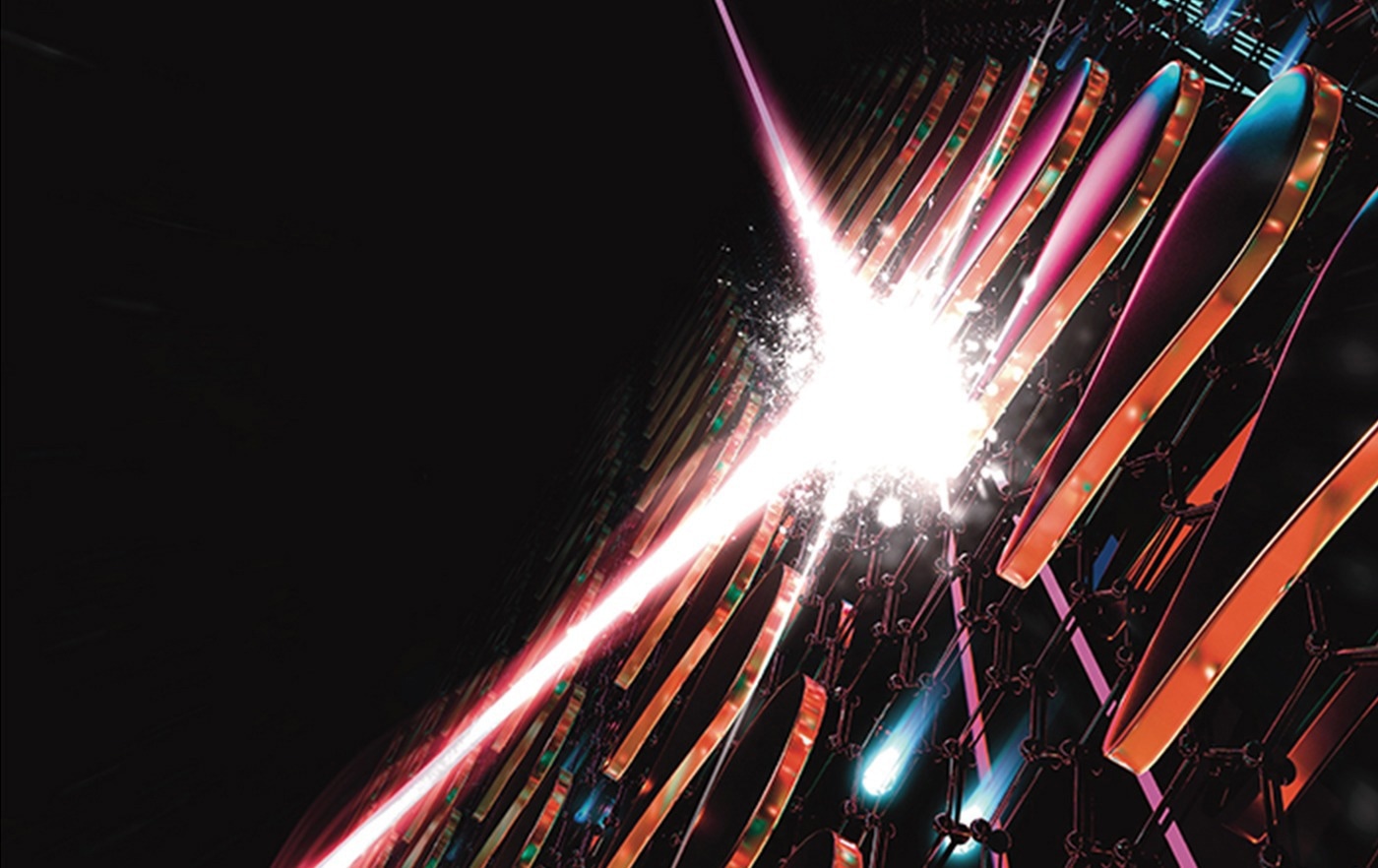
Nanoantennas capture and focus light
According to their latest opinion Nature In the paper, the researchers developed and fabricated asymmetric, nanoscale gold materials on an atomically thin layer of graphene. The gold structures are called „nanoantennas” because they collect and focus light waves, resulting in optical „hot spots” that excite electrons in the graphene. Only the graphene electrons near the hot spots are excited, whereas the rest of the graphene is much less excited.
The researchers used gold nanoantennas in the shape of a teardrop, where one direction in the structure is defined by a reversal symmetry break. Only the sharp points of the nanoantennas contain hot spots, which form a channel for the excited hot electrons to flow along the net direction. This charge current can be controlled and tuned at the nanoscale by inducing various combinations of hot spots.
These metasurfaces provide an easy way to control the amplitude, location, and direction of hot spots and nanoscale charge current with response speeds faster than a picosecond. Then you can think about more detailed activities.
Hu-Tong Chen, Scientist, Center for Integrative Nanotechnologies, Los Alamos National Laboratory
Promising applications for controllable, adjustable charge current
There are many potential applications for the proof-of-concept of these optoelectronic metasurfaces. A naturally occurring charge current can be used as a signal for photodetection; This is particularly noticeable in the long-wavelength infrared region.
The device can generate terahertz radiation, which is helpful for various tasks such as high-speed wireless communications and material characterization using spectroscopy. Additionally, the technique could present new ways to manipulate nanomagnetism, as specific currents can be tailored to generate flexible, nanoscale magnetic fields.
Ultrafast information processing, including computing and microelectronics, can also benefit from increased capabilities. When laser pulses and metasurfaces are used for adaptive circuits, transistor-based computer and electronic designs are rendered slower and less flexible. Adaptive structured light fields, in contrast to traditional circuits, can open up entirely new design options.
Pettin concluded, “These results lay the foundation for versatile patterning and optical control over nanoscale currents. With valuable applications in the laboratory, vectorial metasurfaces can enable advances in a variety of technological domains.„
The Laboratory Directed Research and Development Program of Los Alamos National Laboratory provided funding for the study. The US DOE Office of Science operates the Center for Integrated Nanotechnologies, an Office of Science User Facility.
Journal Note:
Pettin, J., At you (2024) Light-driven vector currents at the nanoscale. Nature. doi:10.1038/s41586-024-07037-4
Source: https://www.lanl.gov/

„Oddany rozwiązywacz problemów. Przyjazny hipsterom praktykant bekonu. Miłośnik kawy. Nieuleczalny introwertyk. Student.