Alex Keita’s Columbia University lab has demonstrated a method for „unchipping” atomically sharp features in 2D hexagonal boron nitride using mid-IR light from a tabletop laser system. [Image: Gaeta Lab / Columbia Engineering]
The ability to etch or pattern nanostructures in various materials opens doors across electronics and photonics, enabling new plasmonic devices and metamaterials. But the techniques for creating such nanopatterns—electron-beam lithography, chemical etching, and femtosecond laser writing—aren’t exactly the stuff of weekend hobbies. Conversely, these approaches typically require multistep processing in expensive cleanroom systems. They can also damage specimens and leave residue or debris in their wake.
Now, Alexander Keita’s lab at Columbia University in the US has devised a way to create at least one type of nanopatterning—direct, nuclear-sharp cuts in a 2D material—using only a mid-IR laser in the gap (Sci. Adv., doi: 10.1126/sciadv.adi3653) to pull off this neat trick, the team carefully tuned the laser to wildly excite the vibrational resonance phonons in the material, causing a straight, atomically precise crack to form and propagate throughout the material. The result? sharp, nanoscale features; No need for a clean room.
The team calls the technique „unzipping.” A remarkable feature is the nanometer-scale sharpness of the cracks it creates, which is orders of magnitude smaller than the mid-IR wavelength of the driving laser. „Typically, you need a shorter wavelength to create a smaller pattern,” Columbia graduate student Cecilia Chen, who led the work, said in a press release describing it. „Here, very sharp nanostructures can be created using very long wavelengths. It’s a paradoxical phenomenon.”
becomes zero in hBN
The layered 2D material chosen by Chen and team as the test bed for the unchipping technique is hexagonal boron nitride (hBN). With a long pedigree as an additive in lubricants and cosmetics, this substance has recently attracted interest. A promising photonic and optoelectronic materialAnother 2D material, graphene, is a substrate for many linear-optical applications.
A remarkable feature of the technique is the nanometer-scale sharpness of the cracks it produces, orders of magnitude smaller than the mid-IR wavelength of the driving laser.
Some of the energies of hBN relate to strong vibrational (phonon) resonances of its crystal structure at the free-space optical wavelength of 7.3 µm, a region accessible to tablet mid-IR lasers. Actually, at work Released late last year, Keita’s group showed that annealing high-quality hBN flakes with a laser tuned to that wavelength can induce and amplify non-optical phenomena such as four-wave mixing and third-harmonic generation. In that study, the aim was to improve the nonlinear properties of the intact crystal, so the researchers deliberately kept the mid-IR laser intensity below 50 TW/cm.2Estimated damage threshold for hBN.
Driving hard stuff
In the new study led by Chen, the team wanted to find out if they could use the same mid-IR resonances to actually modify hBN crystals. To do so, they set up a similar test setup and then drove the laser hard enough to pass the damage threshold.
Specifically, the team integrated a Ti:sapphire mode-locked oscillator, a chirped-pulse amplifier, an optical parametric amplifier, and a difference-frequency generation module in a tablet system to generate a 120-fs, 7.3-µm-wavelength. pulses at a repetition rate of 1 kHz. The pulsed beam was reflected through a 40× microscope objective and focused to an intensity of 50 to 65 TW/cm.2 in ultra-high-purity hBN sample. An adjustable electronic shutter along the beam path allows the team to further control the number of pulses reaching the sample.
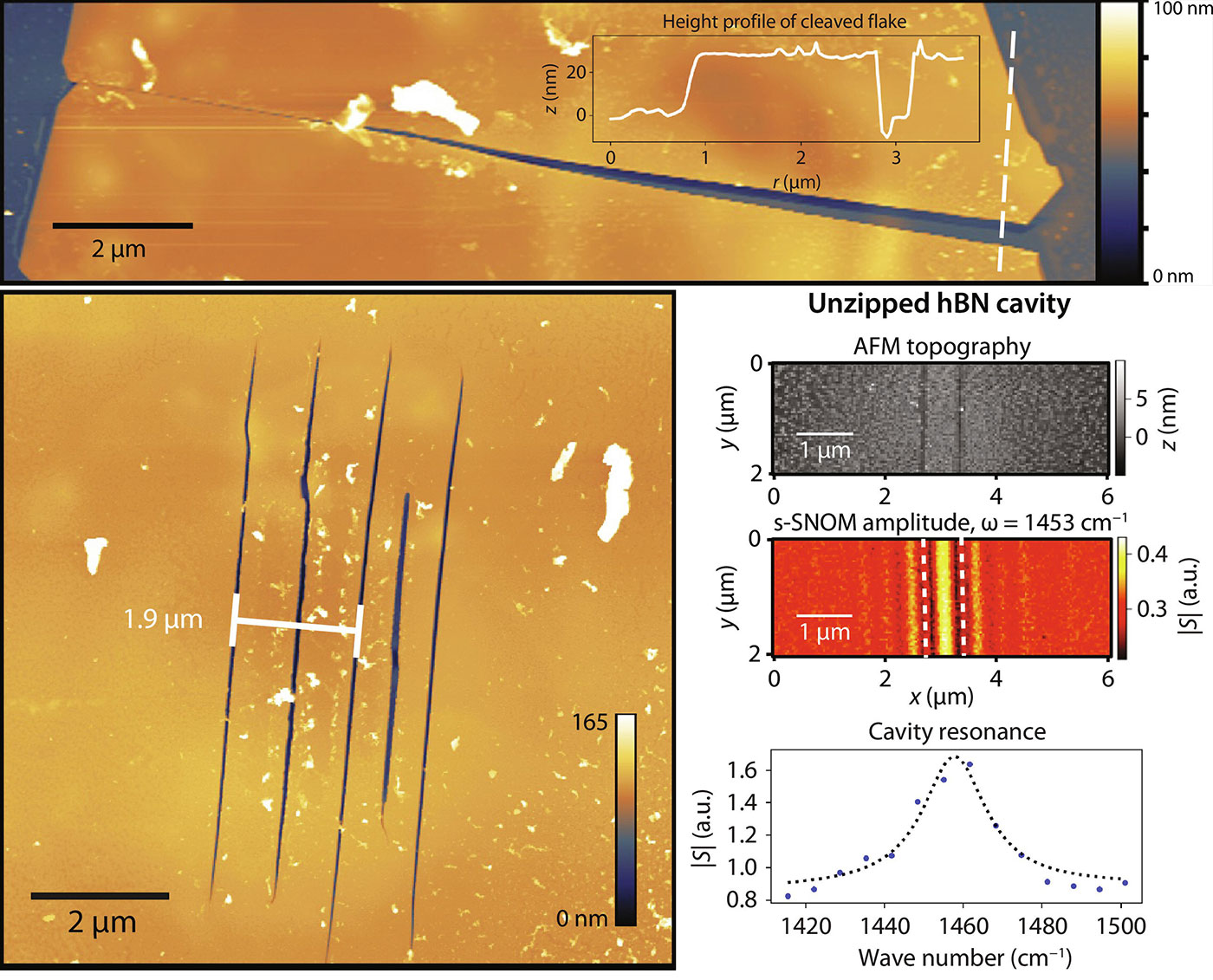
AFM images show examples of nanoscale features enabled by the mid-IR unchipping technique, including long linear cracks (top), a quasi-periodic grating structure (bottom left), and a two-crack Fabry-Perot cavity for phonon confinement and amplification. Poles (bottom right) [Image: C.Y. Chen et al., Sci. Adv., doi: 10.1126/sciadv.adi3653 (2024); CC BY-NC 4.0]
The laser treatment led to the seeding of a crack at the laser spot—probably as a result of an internal defect in the hBN crystal—which induced rapid, “mostly unidirectional” crack-tip propagation through the crystal. The researchers were able to watch the process unfold in real time with a microscope, and estimated the speed of crack propagation to be 100 µm/s.
Atomic-force microscopy and atomic-scale lateral force microscopy confirmed that the resulting features are atomically sharp. The team found that the technique’s effectiveness lies not only in carefully adjusting the laser wavelength, but also (unsurprisingly) in precisely aligning the laser’s polarization to take advantage of the crystal’s symmetrical structure.
Escape from the clean room?
Using a mid-IR tablet laser to create nanometer-scale features is undoubtedly a great achievement. But what is it useful for?
At the very least, Chen and his colleagues hope to provide a new, cleanroom-free method to etch hBN for use in heterostructures. In fact, researchers report that by irradiating adjacent areas with laser light of different polarizations, they can enable more complex, custom wafer shapes for applications such as semiconductor mask patterning. The team also showed that the technique can be used to create quasi-periodic grating structures in hBN.
Perhaps most intriguing are some possible applications in creating phonon polaritons – resonant quasiparticles that arise from the coupling of photons and optical phonons. These quasiparticle methods hold promise in a variety of areas, including diffraction-limit imaging, some quantum applications, and the miniaturization of optical devices. The team’s experiments suggest that infrared illumination can more efficiently excite these useful quasiparticles at the ultrasharp boundaries created by the unchipping method than at the natural edges of a conventional hBN flake. In one model, the team was able to create a Fabry-Perot cavity to confine and amplify such phonon polaritons by decoupling two lines in parallel.

Graduate student Cecilia Chen led the research. [Image: Columbia Engineering]
There’s still plenty of room to improve the technique, Chen noted in a press release accompanying the research. In particular, the unchipping process is very delicate, requiring a carefully tuned laser and precise orientation for optimal results. This, now, is specific to hBN, the 7.3-µm-wavelength resonance of that material.
However, different lasers allow the process to be exported to other materials. On that topic, silicon carbide (SiC)—an increasingly important material for quantum applications and the electrification of society, but difficult to process—is, like hBN, a polar crystal with IR-active optics. Phonons have a resonance wavelength of about 10 µm. Perhaps, with the right laser, unchipping can also become part of the SiC-processing toolkit.

„Oddany rozwiązywacz problemów. Przyjazny hipsterom praktykant bekonu. Miłośnik kawy. Nieuleczalny introwertyk. Student.